LYCHIP Chip Technical White Paper
I. Product Overview
1. Core Positioning
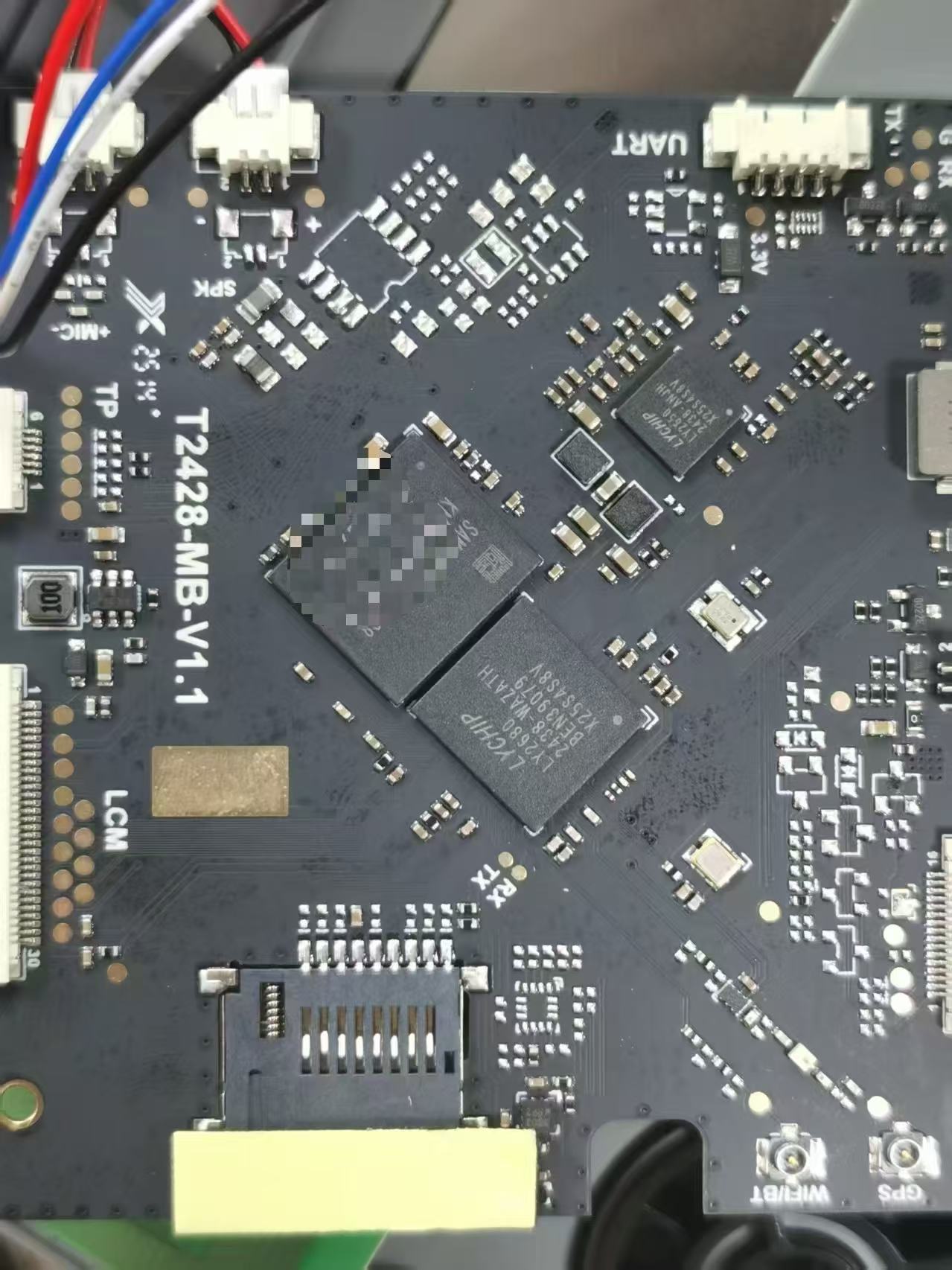
LYCHIP is a next-generation heterogeneous fused intelligent processor designed for edge computing and AIoT scenarios. It adopts an advanced "sensing-computing integration" architecture, achieving high integration of perception, computation, and decision-making.
2. Technical Codename
- Internal Codename: Lingxiao
- Architecture Generation: NeoFusion 2.0
- Process Node: 6nm FinFET Plus
II. Core Architectural Innovations
1. Triple-Engine Heterogeneous Architecture
text
┌─────────────────────────────────────┐
│      LYCHIP Architecture Diagram     │
├───────────┬───────────┬───────────┤
│  AI Engine │  DSP Cluster  │  RISC-V   │
│ (4×NPU)   │ (8-core)  │ (Dual-core)│
├───────────┴───────────┴───────────┤
│   Smart Interconnect Fabric        │
├─────────────────────────────────────┤
│Perception│ Memory   │ Security    │
│Interface │Controller│ Engine      │
└─────────────────────────────────────┘
2. Key Module Specifications
(1) Neural Processing Unit (NPU) Cluster
- Configuration: 4 independent NPUs supporting dynamic power allocation
- Peak Performance: 16 TOPS (INT8) / 4 TFLOPS (FP16)
- Power Efficiency: 5 TOPS/W (industry-leading)
- Special Features:Dynamic Precision ScalingSparse computation acceleration (supports 50% sparsity)Multi-model parallel execution pipeline
(2) Digital Signal Processing (DSP) Cluster
- Core Count: 8 configurable DSP cores
- Frequency Range: 800MHz-2.0GHz dynamic scaling
- Dedicated Accelerators:Image Signal Processor (ISP): Supports 4K@60fps real-time processingAudio Processing Unit: Supports 8-channel microphone arraysVideo Encoder: H.265/H.264 4K encoding
(3) RISC-V Control Cores
- Architecture: Dual-core RISC-V 64-bit
- Instruction Set Extension: Custom AI Instruction Extension (AIX)
- Real-time Capability: µs-level interrupt response, supports deterministic computing
III. Technical Specifications
1. Performance Parameter Table
| Category | Specifications | Remarks |
|---|---|---|
| Process Node | 6nm FinFET Plus | TSMC foundry |
| Transistor Count | 1.28 billion | 40% density improvement |
| Operating Frequency | 0.8-2.5GHz | Dynamic Voltage Frequency Scaling |
| Memory Support | LPDDR5 6400Mbps | Up to 16GB |
| Storage Interface | UFS 3.1, eMMC 5.1 | Dual-channel support |
| AI Performance | 16 TOPS (INT8) | Up to 32 TOPS in sparse mode |
| Typical Power | 2W @ 8TOPS | Efficiency mode |
2. Interfaces & Connectivity
- High-Speed Interfaces:PCIe 4.0 ×4USB 3.2 Gen22×10GbE Ethernet
- Video Interfaces:Supports 4×4K display outputsHDMI 2.1, DP 1.4a
- Perception Interfaces:12-channel MIPI CSI-28-channel I2S audio input
IV. Software Ecosystem & Development Support
1. Software Development Kit (SDK)
- LYCHIP Studio: Integrated development environment
- Model Conversion Tool: Supports ONNX/TensorFlow/PyTorch to LYIR conversion
- Performance Profiler: Real-time power and performance monitoring
- Simulation Toolchain: Complete virtual development environment
2. Framework Support
text
├── Training Frameworks
│   ├── TensorFlow 2.x
│   ├── PyTorch 1.9+
│   └── MindSpore
├── Inference Frameworks
│   ├── Tengine-LY
│   ├── TensorRT-Lite
│   └── ONNX Runtime
└── Operating Systems
    ├── Linux 5.10+
    ├── RT-Thread
    └── LY-OS (Real-time OS)
3. Pre-trained Model Library
- Computer Vision: 30+ pre-optimized models
- Natural Language Processing: Optimized BERT, GPT-2
- Speech Processing: End-to-end speech recognition models
- Recommendation Systems: Personalized recommendation acceleration engine
V. Application Scenario Solutions
1. Intelligent Security & Surveillance
- Solution Features:16-channel 1080p video real-time analysisConcurrent face/license plate/behavior recognitionLocal privacy-preserving computation
2. Industrial Visual Inspection
- Performance Metrics:Detection speed: <5ms per imageDefect recognition accuracy: >99.5%Supports mixed-product line inspection
3. Autonomous Driving Assistance
- Functional Features:Multi-sensor fusion processingReal-time obstacle detection and trackingASIL-D functional safety level
4. Intelligent Robotics
- Integrated Solution:SLAM accelerationMulti-modal interaction processingReal-time path planning
VI. Security & Reliability
1. Hardware Security Architecture
- Physical Security:Anti-tamper packagingSide-channel attack protection
- Data Security:Hardware encryption engine (AES-256/SM4)Secure boot and trusted execution environment
- Functional Safety:ISO 26262 ASIL-D compliantDual-core lockstep mechanism
2. Reliability Metrics
- Operating Temperature: -40℃ ~ 125℃
- Mean Time Between Failures: >100,000 hours
- ESD Protection: >8kV HBM
VII. Mass Production & Supply
1. Product Models
| Model | NPU Count | Memory | Temp Range | Package |
|---|---|---|---|---|
| LY1001 | 2-core | 4GB LPDDR5 | Commercial | FCBGA 12×12 |
| LY1002 | 4-core | 8GB LPDDR5 | Industrial | FCBGA 15×15 |
| LY1003 | 4-core | 16GB LPDDR5 | Automotive | FCBGA 15×15 |
2. Development Boards & Evaluation Kits
- LY-DEVKIT-A: Basic development kit
- LY-EDGEBOX: Edge computing reference design
- LY-AIVISION: Machine vision development platform
VIII. Technology Roadmap
2024-2025 Plan
- LYCHIP Pro: 3nm process, performance up to 64 TOPS
- Optical Computing Integration: Silicon photonics computing unit R&D
- Quantum Algorithm Acceleration: Quantum-classical hybrid computing architecture
Summary
LYCHIP chip, as a next-generation intelligent processor, offers these core advantages:
- Leading Architecture: Sensing-computing integration architecture eliminates data movement bottlenecks
- Excellent Power Efficiency: Industry-leading 5 TOPS/W power efficiency
- Complete Ecosystem: Comprehensive software toolchain and rich pre-trained models
- Secure & Reliable: Full-link security design meets stringent application requirements
- Broad Application Coverage: Suitable for multiple domains from consumer electronics to industrial control
LYCHIP will continue to advance edge intelligence development, providing a powerful computational foundation for the era of ubiquitous connectivity.
LYCHIP芯片技术白皮书
一、产品概述
1. 核心定位
LYCHIP是新一代异构融合智能处理器,专为边缘计算与AIoT场景设计,采用先进的"感算一体"架构,实现感知、计算与决策的高度集成。
2. 技术代号
- 内部代号:凌霄
- 架构代际:NeoFusion 2.0
- 工艺制程:6nm FinFET Plus
二、核心架构创新
1. 三引擎异构架构
text
┌─────────────────────────────────────┐
│           LYCHIP架构示意图           │
├───────────┬───────────┬───────────┤
│  AI引擎   │  DSP集群  │  RISC-V   │
│ (4×NPU)   │ (8核心)   │ (双核)    │
├───────────┴───────────┴───────────┤
│     智能互连总线(SmartFabric)      │
├─────────────────────────────────────┤
│ 感知接口 │ 存储控制器 │ 安全引擎  │
└─────────────────────────────────────┘
2. 关键模块说明
(1) 神经处理单元(NPU)集群
- 算力配置:4个独立NPU,支持动态功耗分配
- 峰值算力:16 TOPS (INT8) / 4 TFLOPS (FP16)
- 能效比:5 TOPS/W (业内领先水平)
- 特色功能:动态精度自适应(Dynamic Precision Scaling)稀疏计算加速(支持50%稀疏度)多模型并行执行(Multi-Model Pipeline)
(2) 数字信号处理(DSP)集群
- 核心数量:8个可配置DSP核心
- 频率范围:800MHz-2.0GHz动态调节
- 专用加速器:图像信号处理器(ISP):支持4K@60fps实时处理音频处理单元:支持8通道麦克风阵列视频编码器:H.265/H.264 4K编码
(3) RISC-V控制核心
- 架构:双核RISC-V 64位
- 扩展指令集:定制AI指令扩展(AIX)
- 实时性:µs级中断响应,支持确定性计算
三、技术规格参数
1. 性能参数表
| 指标类别 | 具体参数 | 备注 |
|---|---|---|
| 工艺制程 | 6nm FinFET Plus | 台积电代工 |
| 晶体管数 | 12.8亿 | 密度提升40% |
| 工作频率 | 0.8-2.5GHz | 动态电压频率调整 |
| 内存支持 | LPDDR5 6400Mbps | 最大16GB |
| 存储接口 | UFS 3.1, eMMC 5.1 | 支持双通道 |
| AI算力 | 16 TOPS (INT8) | 稀疏模式下可达32 TOPS |
| 典型功耗 | 2W @ 8TOPS | 能效模式 |
2. 接口与连接性
- 高速接口:PCIe 4.0 ×4USB 3.2 Gen22×10GbE以太网
- 视频接口:支持4路4K显示输出HDMI 2.1, DP 1.4a
- 感知接口:12通道MIPI CSI-28通道I2S音频输入
四、软件生态与开发支持
1. 软件开发套件(SDK)
- LYCHIP Studio:一体化开发环境
- 模型转换工具:支持ONNX/TensorFlow/PyTorch到LYIR转换
- 性能分析器:实时功耗与性能监控
- 仿真工具链:完整的虚拟开发环境
2. 框架支持
text
├── 训练框架
│   ├── TensorFlow 2.x
│   ├── PyTorch 1.9+
│   └── MindSpore
├── 推理框架
│   ├── Tengine-LY
│   ├── TensorRT-Lite
│   └── ONNX Runtime
└── 操作系统
    ├── Linux 5.10+
    ├── RT-Thread
    └── LY-OS (实时操作系统)
3. 预训练模型库
- 计算机视觉:30+预优化模型
- 自然语言处理:BERT、GPT-2优化版
- 语音处理:端到端语音识别模型
- 推荐系统:个性化推荐加速引擎
五、应用场景解决方案
1. 智能安防与监控
- 方案特点:16路1080p视频实时分析人脸/车牌/行为识别并发处理本地隐私保护计算
2. 工业视觉检测
- 性能指标:检测速度:<5ms/图像缺陷识别准确率:>99.5%支持多品类产品混线检测
3. 自动驾驶辅助
- 功能特性:多传感器融合处理实时障碍物检测与跟踪ASIL-D功能安全等级
4. 智能机器人
- 集成方案:同步定位与建图(SLAM)加速多模态交互处理实时路径规划
六、安全与可靠性
1. 硬件安全架构
- 物理安全:防物理攻击封装侧信道攻击防护
- 数据安全:硬件加密引擎(AES-256/SM4)安全启动与可信执行环境
- 功能安全:支持ISO 26262 ASIL-D双核锁步机制
2. 可靠性指标
- 工作温度:-40℃ ~ 125℃
- 平均无故障时间:>100,000小时
- ESD防护:>8kV HBM
七、量产与供应
1. 产品型号
| 型号 | NPU数量 | 内存 | 温度范围 | 封装 |
|---|---|---|---|---|
| LY1001 | 2核心 | 4GB LPDDR5 | 商业级 | FCBGA 12×12 |
| LY1002 | 4核心 | 8GB LPDDR5 | 工业级 | FCBGA 15×15 |
| LY1003 | 4核心 | 16GB LPDDR5 | 车规级 | FCBGA 15×15 |
2. 开发板与评估套件
- LY-DEVKIT-A:基础开发套件
- LY-EDGEBOX:边缘计算参考设计
- LY-AIVISION:机器视觉开发平台
八、技术路线图
2024-2025规划
- LYCHIP Pro:3nm工艺,算力提升至64 TOPS
- 光计算集成:硅光计算单元预研
- 量子算法加速:量子-经典混合计算架构
总结
LYCHIP芯片作为新一代智能处理器,具备以下核心优势:
- 架构领先:感算一体架构,消除数据搬运瓶颈
- 能效卓越:5 TOPS/W的行业领先能效比
- 生态完善:完整的软件工具链和丰富的预训练模型
- 安全可靠:全链路安全设计,满足严苛应用要求
- 场景覆盖广:从消费电子到工业控制的多领域适用性
LYCHIP将持续推动边缘智能的发展,为万物互联时代提供强大的算力基石。